The successful integration of a sub-0.5nm dielectric with 2D semiconductors

Field-effect transistors (FETs) are transistors in which the resistance of most of the electrical current can be controlled by a transverse electric field. Over the past decade or so, these devices have proved to be very valuable solutions for controlling the flow of current in semiconductors.
To further develop FETs, electronics engineers worldwide have recently been trying to reduce their size. While these down-scaling efforts have been found to increase the device’s speed and lower the power consumption, they are also associated with short-channel effects (i.e., unfavorable effects that occur when an FET’s channel length is approximately equal to the space charge regions of source and drain junctions within its substrate).
These undesirable effects, which include barrier lowering and velocity saturation, could be suppressed by using 2D semiconductor channels with high carrier mobilities and ultrathin high-k dielectrics (i.e., materials with high dielectric constants). Integrating 2D semiconductors with dielectrics with similar oxide thicknesses has been found to be highly challenging.
Researchers at Peking University and University of Texas at Austin have recently demonstrated the successful integration of a sub-0.5nm dielectric layer with 2D semiconductor-based transistors. Their design, introduced in a paper published in Nature Electronics, could ultimately pave the way towards the development of smaller, faster, and more efficient FETs.
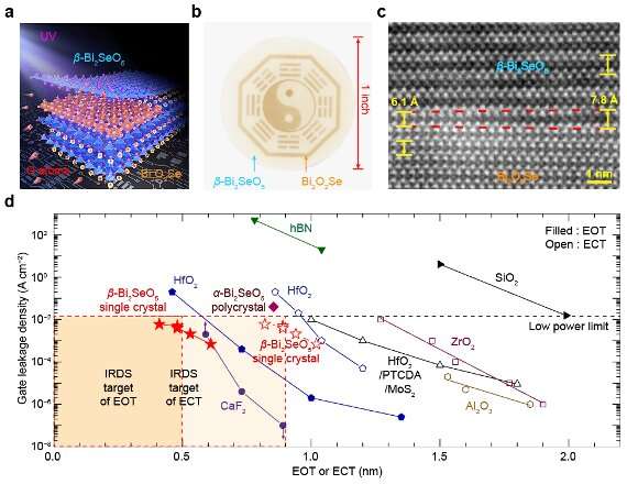
“Previously we have synthesized a poly-crystalline high-κ (dielectric constant) native oxide dielectric of 2D Bi2O2Se and found that its equivalent oxide thickness (EOT) can be scaled down to 0.9 nm, but the leakage current exceeds the low-power limit,” Hailin Peng, one of the researchers who carried out the study, told TechXplore. “Inspired by the layered crystal structure of 2D Bi2O2Se and the intercalation of 2D materials, we designed an intercalative oxidation process to retain the lattice framework of the precursor, to obtain a single-crystalline native oxide with better insulativity for further downscaling.”
To integrate their dielectric with 2D semiconductors, Peng and his colleagues used a process called UV-assisted intercalative oxidation. Firstly, they decomposed oxygen molecules contained in the air into atomic oxygen using 185 nm ultraviolet (UV) rays emitted from a low-pressure mercury lamp.
Subsequently, they used the atomic oxygen to oxidize the Se2- layer in the 2D semiconductor Bi2O2Se between the two [Bi2O2]n2n+ layers, without affecting the properties of the [Bi2O2]n2n+ layers. This process led to the formation of a new ‘layered phase,” which inherited the single-crystalline [Bi2O2]n2n+ structure of the original Bi2O2Se sample.
“The as-synthesized oxide is further confirmed to be a single-crystalline native dielectric and named β-Bi2SeO5,” Peng explained. “The single-crystalline native oxide β-Bi2SeO5 has a thickness-independent high dielectric constant of about 22, ultraflat lattice-matched interface, and excellent insulativity. Even when scaled down to 2.3 nm and the EOT (equivalent oxide thickness, 3.9×thickness/dielectric constant) is as low as 0.41 nm, the leakage current at 1 V gate voltage is still below the low-power limit (0.015 A/cm2), meeting the industrial requirements of dielectrics in next-generation transistors.”
The initial tests carried out by Peng and his colleagues yielded interesting results. Overall, their findings suggest β-Bi2SeO5, the material they created, could be promising for developing an ultrathin high-κ (dielectric constant) gate dielectric in 2D transistors.
“The most notable achievement of our study was the successful integration of sub-0.5-nm-EOT dielectrics in top-gated 2D transistors, which meets the benchmarks of dielectric in the 2021 International Roadmap for Devices and Systems,” Peng said. “Thus, one of the challenges for 2D electronics, the integration with sub-0.5-nm-EOT ultrathin high-κ dielectric, has been overcome.”
This team of researchers demonstrated the possibility of integrating 2D semiconductors with high-k dielectrics. In the future, the material that they created and the method introduced in their paper could be used to create smaller and highly-performing FETs that are not adversely impacted by short-channel effects.
“We will now further investigate the compatibility of β-Bi2SeO5 with other common 2D materials and metal electrodes,” Peng added. “In addition, a large-scale transfer process of Bi2SeO5 or its precursor Bi2O2Se is also desired for the integration of this ultrathin high-κ dielectric with a broad range of 2D materials.”
A new native oxide high-k gate dielectric for fabricating 2-D electronics
Yichi Zhang et al, A single-crystalline native dielectric for two-dimensional semiconductors with an equivalent oxide thickness below 0.5 nm, Nature Electronics (2022). DOI: 10.1038/s41928-022-00824-9
Tianran Li et al, A native oxide high-κ gate dielectric for two-dimensional electronics, Nature Electronics (2020). DOI: 10.1038/s41928-020-0444-6
© 2022 Science X Network
Citation:
The successful integration of a sub-0.5nm dielectric with 2D semiconductors (2022, October 17)
retrieved 17 October 2022
from https://techxplore.com/news/2022-10-successful-sub-05nm-dielectric-2d-semiconductors.html
This document is subject to copyright. Apart from any fair dealing for the purpose of private study or research, no
part may be reproduced without the written permission. The content is provided for information purposes only.
For all the latest Technology News Click Here
For the latest news and updates, follow us on Google News.
