Electronic metadevices break barriers to ultra-fast communications

EPFL researchers have come up with a new approach to electronics that involves engineering metastructures at the sub-wavelength scale. It could launch the next generation of ultra-fast devices for exchanging massive amounts of data, with applications in 6G communications and beyond.
Until now, the ability to make electronic devices faster has come down to a simple principle: scaling down transistors and other components. But this approach is reaching its limit, as the benefits of shrinking are counterbalanced by detrimental effects like resistance and decreased output power.
Elison Matioli of the Power and Wide-band-gap Electronics Research Lab (POWERlab) in EPFL’s School of Engineering explains that further miniaturization is therefore not a viable solution to better electronics performance. “New papers come out describing smaller and smaller devices, but in the case of materials made from gallium nitride, the best devices in terms of frequency were already published a few years back,” he says. “After that, there is really nothing better, because as device size is reduced, we face fundamental limitations. This is true regardless of the material used.”
In response to this challenge, Matioli and Ph.D. student Mohammad Samizadeh Nikoo came up with a new approach to electronics that could overcome these limitations and enable a new class of terahertz devices.
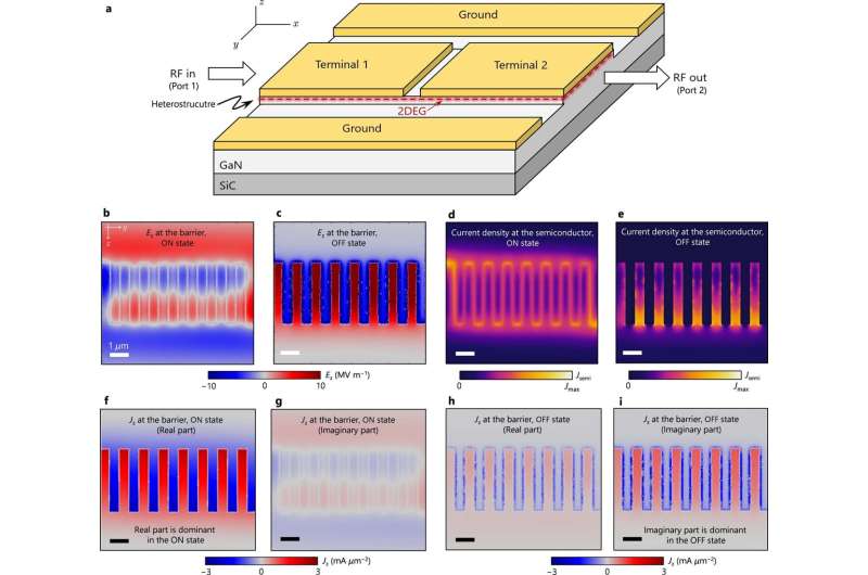
Instead of shrinking their device, they rearranged it, notably by etching patterned contacts called metastructures at sub-wavelength distances onto a semiconductor made of gallium nitride and indium gallium nitride. These metastructures allow the electrical fields inside the device to be controlled, yielding extraordinary properties that do not occur in nature.
Crucially, the device can operate at electromagnetic frequencies in the terahertz range (between 0.3 and 30 THz)—significantly faster than the gigahertz waves used in today’s electronics. They can therefore carry much greater quantities of information for a given signal or period, giving them great potential for applications in 6G communications and beyond.
“We found that manipulating radiofrequency fields at microscopic scales can significantly boost the performance of electronic devices, without relying on aggressive downscaling,” explains Samizadeh Nikoo, who is the first author of an article on the breakthrough recently published in the journal Nature.
Record high frequencies, record low resistance
Because terahertz frequencies are too fast for current electronics to manage, and too slow for optics applications, this range is often referred to as the “terahertz gap.” Using sub-wavelength metastructures to modulate terahertz waves is a technique that comes from the world of optics. But the POWERlab’s method allows for an unprecedented degree of electronic control, unlike the optics approach of shining an external beam of light onto an existing pattern.
“In our electronics-based approach, the ability to control induced radiofrequencies comes from the combination of the sub-wavelength patterned contacts, plus the control of the electronic channel with applied voltage. This means that we can change the collective effect inside the metadevice by inducing electrons (or not),” says Matioli.
While the most advanced devices on the market today can achieve frequencies of up to 2 THz, the POWERlab’s metadevices can reach 20 THz. Similarly, today’s devices operating near the terahertz range tend to break down at voltages below 2 volts, while the metadevices can support over 20 volts. This enables the transmission and modulation of terahertz signals with much greater power and frequency than is currently possible.
Integrated solutions
As Samizadeh Nikoo explains, modulating terahertz waves is crucial for the future of telecommunications, as the increasing data requirements of technologies like autonomous vehicles and 6G mobile communications are fast reaching the limits of today’s devices. The electronic metadevices developed in the POWERlab could form the basis for integrated terahertz electronics by producing compact, high-frequency chips that can already be used with smartphones, for example.
“This new technology could change the future of ultra-high-speed communications, as it is compatible with existing processes in semiconductor manufacturing. We have demonstrated data transmission of up to 100 gigabits per second at terahertz frequencies, which is already 10 times higher than what we have today with 5G,” Samizadeh Nikoo says.
To fully realize the potential of the approach, Matioli says the next step is to develop other electronics components ready for integration into terahertz circuits.
“Integrated terahertz electronics are the next frontier for a connected future. But our electronic metadevices are just one component. We need to develop other integrated terahertz components to fully realize the potential of this technology. That is our vision and goal.”
More information:
Mohammad Samizadeh Nikoo et al, Electronic metadevices for terahertz applications, Nature (2023). DOI: 10.1038/s41586-022-05595-z
Citation:
Electronic metadevices break barriers to ultra-fast communications (2023, February 17)
retrieved 17 February 2023
from https://techxplore.com/news/2023-02-electronic-metadevices-barriers-ultra-fast-communications.html
This document is subject to copyright. Apart from any fair dealing for the purpose of private study or research, no
part may be reproduced without the written permission. The content is provided for information purposes only.
For all the latest Technology News Click Here
For the latest news and updates, follow us on Google News.
